Copper and Nanotechnology
Copper Applications in Innovative Technology Area
Introduction | Copper's Role in Today's Applications | Tomorrow's Applications | Conclusions | About the Author | References
Introduction 
"Nanotechnology" has become the modern day buzzword in new technological development. It describes many types of research in which the characteristic dimensions of the materials of interest are less than about a micron, or 1,000 nanometers (nm). A nanometer is one billionth of a meter (0.000,000,00 1 m).
Nanotechnology, therefore, involves nanoparticles and nanostructures. Nanoparticles may be individual sub-micron particles of a metal, a metal oxide or an organic complex of a metal. The previous name for this state of matter was colloid. Colloidal-size metal and semiconductor materials in the 1 nm to 20 nm range have been an intriguing area of materials research in that they represent a transition range between molecular and bulk properties. In this size range, unique physical, optical and electronic properties are said to be exhibited that are not present in the bulk phase.
Nanoparticles can be formed by a variety of methods, such as precipitation from an aqueous solution, electrolysis from an aqueous solution, vapor deposition on a substrate or sputtering from a metal wire or plate. Nanostructures are complex microscopic arrangements: tubes, plates or even electronic circuits such as those formed on computer chips.
Companies, universities and government laboratories are aggressively exploring new ways of forming nanoparticles and nanostructures, characterizing their properties and exploring for new applications for them. The number of issued patents involving nanotechnology is increasing rapidly - from 370 in 1997 to 2,650 in 2002. While only 2% of all patents issued in 2002 involved nanotechnology, that was much higher than the 0.3% in 1997. About 90% of the applications came from private corporations, while universities filed roughly 7%, and about 3% were filed by government agencies and collaborative research centers 1 .
According to experts in the field, nanotechnology will have an impact on the global economy of more than $1 trillion within a decade. Even though its commercialization may seem far off at times, nanotechnology is projected to have huge effects on many practical industries, including manufacturing, health care, energy, agriculture, communications, transportation and electronics. For example, nanotechnology is projected to make possible the manufacturer of such mundane products as corrosion-resistant paint, spill-resistant blue jeans and a super mouthwash that would eliminate the need for brushing and flossing. In addition, it is expected to spawn entirely new industries.
To assist in the development of nanotechnology the Congress has passed the Nanotechnology Research Act of 2003 and the U.S. government has formed The National Nanotechnology Initiative (NNI) 2 . This is a federal R&D program established to coordinate the multi-agency efforts in accelerating the development of nanoscale science, engineering and technology. Spending for the NNI in FY 2005 is programmed at $1.1 billion. The major agencies involved are the National Science Foundation, the Department of Defense, the Department of Energy, the National Institutes of Health and the National Institute for Standards and Technology. However, 17 other agencies also have nanotechnology programs underway. There are similar programs in a number of other countries including China, Germany, Japan and Russia.
There are a number of methods of producing nanoparticles of copper; however, the stability and reactivity of copper are the two main factors that impede the use of the material. Thus synthesizing the stable copper nanoparticles is the challenge and the subject of much research. While the role copper will finally play in nanotechnology is yet to be determined, the metal is already filling a number of notable applications. In addition, there are a number of recent technical developments that indicate promise for expansion of copper's role in nanotechnology.
Copper's Role in Today's Applications
Nanocopper Particles as an Algaecide, Fungicide and Other Uses
Colloidal copper (nanocopper particles suspended in water) has been used since at least 1931, in a product known as Bouisol 3 , as fungicide in the growing of grapes, fruit trees, etc. and as an algaecide in the treatment of water in swimming pools. It is also sold in health food stores as a means of supplementing the copper in one's diet. However, while it is known that the body requires copper as a nutritional trace element, there is no indication that acquiring that copper as a colloid is any better than acquiring it in ionic form. In fact, at least one colloidal copper manufacturer has been cited for violating the Pure Food and Drug Act for citing health benefits in his advertisements 4 . In addition, nanosized copper particles are currently sold for application in polymers and plastics, lubricants, inks and metallic coatings 5 .Copper Interconnects for Computers
Continued improvements in lithography have resulted in line widths that are less than one micron, thus classifying computer chips as an example of nanotechnology. The use of copper interconnects on silicon chips for use in personal computers is the first and most widespread use of copper in nanotechnology. It is this technology that has made it possible for personal computers to achieve speeds in the gigahertz range 6 .The most widely used type of integrated circuit (IC) used today for both processor and memory in PCs as well as mainframes is the complimentary metal oxide semiconductor (CMOS). Traditional CMOSs have been based on aluminum conductors and a silica (SiO2) dielectric. As devices become faster and more complicated the conductors on the chip must occupy less and less space and therefore become narrower and narrower. This narrowing of the conductor causes an increase in the Resistance-Capacitance (RC) delay. The RC delay, combined with the gate delay, the delay inherent to the logic circuit to which the conductors are attached, is the interconnect delay that controls the speed of the computer.
The industry faced a difficult future as it considered devices having conductors less than 0.25 microns in width. From the beginning, it was clear that copper would have a decided advantage over aluminum, the commonly used conductor in an integrated circuit (IC). This is due to copper's higher electrical conductivity compared with that of aluminum (Copper has about two-thirds the electrical resistance of aluminum on a volumetric basis). Figure 1 shows the theoretical advantage of copper over aluminum in an interconnect by virtue of fine dimensions possible with copper 7 . Copper, in a low K dielectric interconnect at 0.1 microns width will offer approximately the same delay as an aluminum/SiO2 interconnect at 0.25 microns width.
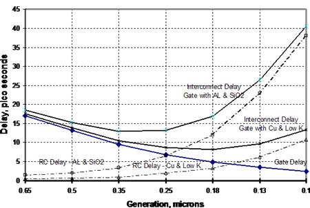 Figure 1. Theoretical Speed/Performance Relationship Showing Effect of Size of Conductor. (Source: Bohr, Mark T., "Interconnect Scaling - The Real Limiter to High Performance ULSI," Proceedings of the 1995 IEEE International Electron Devices Meeting, pp 241-242.)
However, copper was difficult to use since it reacted with the silicon substrate. IBM's development of the Double Damascene Process, whereby a tantalum diffusion barrier was laid down under the copper, enabled copper to enter this application. In this process, copper is applied to the substrate by a vacuum deposition process in which one of two types of copper targets are used, as shown in Figures 2 and 3. The copper in these targets is 99.999 to 99.9999% pure.
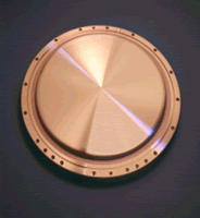 Figure 2. Applied Materials SIB Copper Cathode. Figure 2. Applied Materials SIB Copper Cathode. (Photo - Courtesy, Praxair, Inc.) |
 Figure 3. Novellus Hollow Magnetron (HCM). Figure 3. Novellus Hollow Magnetron (HCM). (Photo - Courtesy, Praxair, Inc.) |
The resulting "nanostructure" is an electronic circuit as illustrated in Figure 4.
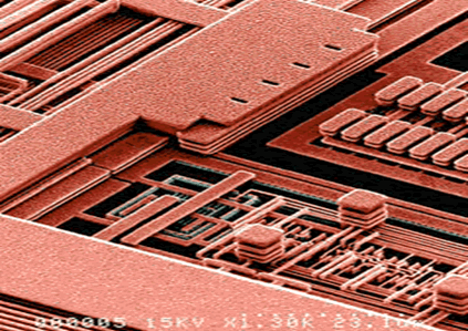 Figure 4. Copper Interconnects. (Photo - Courtesy, Praxair, Inc.)
Coating of Copper Alloy Injection Molds
Nanotechnology is also being used to improve the wear resistance of copper alloy injection molds. This application does not involve copper nanoparticles; rather, it involves treating the wear-prone surface of the copper alloy mold with another nanoparticle - Armaloy XADC, a nodular metallic chromium containing a nano-composite of diamond 8, 9, 10.Tomorrow's Applications
Microelectronics
As discussed above, nanocopper interconnects are currently the mainstay of ICs used in memory and processor chips. In addition, nanocopper/polyimide composites are under study as a dielectric material in micoelectronics 11 .
Heat Transfer Systems
Scientists and engineers have been trying for decades to develop fluids with improved heat transfer characteristics. Such fluids would have application in improving the efficiency of automobiles, heating/air conditioning systems and industrial equipment. Argonne National Laboratory (ANL) has recently developed metal nanofluids based on nanoparticles of copper, Figure 5 12 . Adding only 0.3 volume percent of copper nanoparticles to ethylene glycol increased its thermal conductivity up to 40%. ANL researchers claim that these fluids are one of the world's most advanced heat transfer media, having both ultra-high thermal conductivity and long-term stability.
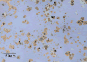 Figure 5. Bright-Field Transmission Electron Microscope (TEM) Micrograph Of Copper Nanoparticles Produced By Direct Evaporation In Ethylene Glycol.
 (Photo - Courtesy, American Chemical Society)
They dramatically enhance heat transfer, and their ability to do so is far superior to that of the best competing fluid (more than 10 times better). And they outperform competing fluids in terms of long-term stability, as well. Argonne's extremely small nanoparticles have been shown to enhance the thermal conductivity of a base fluid dramatically. The enhancement is more than 10 times larger than predicted. Since even a small increase in heat transfer can save pumping power, nanofluids could offer significant savings. Nanofluids with a thermal conductivity of about three times that of a base fluid could double the fluid's heat transfer rate. To double it without adding nanoparticles, pumping power would have to increase tenfold. Metal nanoparticles enhance heat transfer better than oxide nanoparticles.
Preliminary tests show that nanofluids may solve a number of problems plaguing the heating, ventilation and air conditioning (HVAC) industry. But their use could go beyond heat transfer in automobiles and manufacturing equipment. With continued research, Choi and Eastman envision nanofluids improving the efficiency of high-heat flux devices like supercomputers and providing new cancer treatment techniques 13 .
Sorbents - Treatment of Radioactive Waste
In a previous Innovations article, "Will copper Sop Up Radioactive Pollution," a new copper containing sorbent was described as an organic-inorganic nanocomposite that has the ability to sorb radioactive cesium 14, 15.
Research conducted at the Pacific Northwest National Laboratories (PNNL), a DOE facility in Richland, Washington, has created a highly selective sorbent that rapidly removes almost all cesium from aqueous solution. The application for this technology is the retrieval of cesium-137 from nuclear waste and making it available in a clinically useful form, which would therefore benefit both the environment and medical science.
 Figure 6. A Single Pore, In This Case Coated With a Mercaptopropylsiloxy Monolayer, Is Shown In The Background.
 A model of one surfactant molecule is also shown.
(Photo - Courtesy, American Chemical Society)
The technology involves forming a nano-sized copper ferrocyanide complex on the surface of a proprietary mesoporous silicate ceramic, a process known as self-assembled monolayers on mesoporous supports, or SAMMS. Mesoporous refers to the structure of the ceramic's internal cavities. As shown in Figure 6, the pores are tubular, hexagonally close-packed and extremely tiny (20-200 Å in diameter), yielding a material with a surface area of approximately 1000 m²/g. That, according to the author, means five grams of SAMMS powder has a surface area the size of a football field.
To test the cesium-selective sorbent, the PNNL researchers used solutions containing two parts per million (ppm) of cesium, which is similar to the radiocesium concentration of the relevant nuclear waste. They found that the cesium concentration plummeted to less than four parts per billion (ppb) within one minute--that is, more than 99% of the cesium was complexed. Cesium levels declined further - to less than 1 ppb - within 2 hours.
Gas Separation and Storage - Hydrogen
The interest in using hydrogen as an automotive fuel, perhaps by burning in a fuel cell, has lead to the investigation of methods of storing hydrogen at ambient pressure. Groups working at the University of Michigan and the University of Texas have discovered that a metal-organic framework (MOF) compound containing copper can store up to 2.5 wt % hydrogen at 77o K (the temperature of liquid nitrogen) 16, 17. Their compound, MOF - 505, shown in Figure 7, is composed of Cu2(CO2)4 paddle-wheel-shaped units that are joined by biphenyltetracarboxylic acid linker groups.
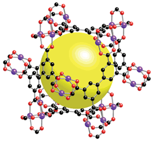 Figure 7. Molecular Structure of University of Michigan MOF-505 Nanostructure. Yellow sphere indicates cavity volume. Copper is blue, Carbon is black and Oxygen is red.
 (Photo - Courtesy, American Chemical Society.)
Acetylene:
A hybrid copper-organic nanostructure developed in Japan is capable of sorbing acetylene in preference to its close molecular cousin, carbon dioxide 18, 19. Thus this development represents a means of both separating acetylene from carbon dioxide and storing it within a solid structure at atmospheric pressure and room temperature. The material is Cu2(pzdc)2 (pyz) - where pzdc is pyrazine-2,3-dicarboxylate and pyz is pyrazine. The effect is illustrated in Figure 8.
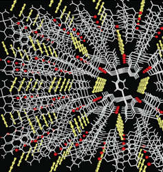 Figure 8. One-Dimensional Channels of Porous Solid Accommodate Acetylene Molecules (yellow).
 (Photo - Courtesy, American Chemical Society)
Antimicrobial Materials
The International Copper Association Ltd. is currently sponsoring a project on nanostructured copper nanoparticles at the Massachusetts Institute of Technology. The focus of the research is the development of a new antimicrobial material. Antibacterial materials are an area of prime interest today in view of the need to control methicillin resistant Staphylococcus aureus (MRSA) infections in hospitals and other health care facilities as well as campylobacteria in food preparation and Aspergillus niger in HVAC systems, among others 20.
Super Strong Materials
Researchers at Johns Hopkins University have announced the development of a form of strong copper that retains its ductility. According to the researchers, by using a unique heat-treating process involving extreme cold (liquid nitrogen) and mechanical manipulation, they can form a copper sheet that has crystallites in the nano size range. This material exhibits unusual stress-strain characteristics. The researchers speculate that when the metallic grains are smaller, more grain boundaries exist to block the moving dislocations and thus the metal's strength is increased 21 . It should be noted, however, that other researchers who have investigated ultrafine grain sizes in copper have noted just the opposite effect; namely, as the grain size approached the nano size range, the strength of the metal began to decrease 22, 23.
Conclusions
The field of nanotechnology is still in its infancy; however, sufficient progress has been made in a number of systems to suggest that there is reason to believe that the field has the potential of spawning many new technologies. The present usage of copper interconnects in integrated circuits is an example of a significant breakthrough in nanotechnology that is already having an impact on all of us. Other potential applications, based on copper, are under development.
About the Author
William H. Dresher has over 30 years experience in corporate and academic management in R&D, in the fields of extractive metallurgy of base and refractory metals, copper processing, products and marketing, as well as expertise in the environmental aspects of copper in health and ecotoxicity. In his career he has been Assistant Director of Research for Union Carbide Corporation's Mining and Metals Division, Dean of the College of Mines of the University of Arizona, President of the International Copper Research Association, Inc. and most recently, the Vice President of Technology of the International Copper Association, Ltd. He is a graduate of Drexel University in Philadelphia with a BS degree in Chemical Engineering and of the University of Utah with a Ph.D. in Metallurgy.
References:
1. Heins, H.H., " Patent Trends in Nanotechnology," Townsend and Townsend and Crew, LLP, September, 2003. ![]()
2. The National Nanotechnology Initiative, Research and Development Leading to a Revolution in Technology and Industry, Supplement to the President's FY 2006 Budget, Office of the President of the United States. ![]()
3. Brouisol. British Patent No. 392556, 1931. ![]()
4. U.S. Department of Health and Human Services letter of December 2, 2004 to Purest Colloids, Inc., Westhampton, N.J. ![]()
5. Canano Technologies, 230 Metcalf Street, P.O. Box 911, Tweed, Ontario, K0K 3J0. ![]()
6. Dresher, W. H., " Speeding up your computer in the 21st Century using Copper ICs," Innovations, Copper Development Association Inc., January 2000. ![]()
7. Bohr, Mark T., Interconnect Scaling-The Real Limiter to High Performance ULSI, Proceedings of the 1995 IEEE International Electron Devices Meeting, pp 241-242. ![]()
8. Armoloy of Western Pennsylvania Inc. 1231 Rodi Road, Turtle Creek, PA 15145. ![]()
9. Engleman, P. and R. Dearly, " Injection Mold Guidelines - Maximizing performance using copper alloys," Copper Development Association Inc., 260 Madison Ave., New York, NY, January 2000, p.50. ![]()
10. Engleman, P., K. Hayden and M. Monfore, " Undercutting Mold Performance: Ejection Wear," Copper Development Association Inc., 260 Madison Ave., New York, NY, 2003. ![]()
11. Michael B. Sullivan, Zhang Jia, Wu Ping, Zheng Jianwei, Zhu Baoku and Xu Zhikang, "Theoretical Study of nano-Copper/Polyimide Composite," Presented: 9th International Conference on Advanced Materials 2005 & 3rd International Conference on Materials for Advanced Technologies 2005, Singapore, 3-8 July 2005. ![]()
12. Choi, S., and J. A. Eastman, "Enhanced Heat Transfer Using Nanofluids," U.S. Pat. No. 6,221,275, April 24, 2001. US Department of Energy, Argonne National Laboratories. ![]()
13. Choi, S., and J. A. Eastman, U.S. Department of Energy, Argonne National Laboratories. ![]()
14. Kundig, K. J.A., " Will Copper Sop Up Radioactive Pollution," Innovations, Copper Development Association Inc., June 2002. ![]()
15. Dagani, R., Silica Sorbents with a Taste for Metals," Chemical and Engineering News, 79, (42), October 15, 2001. American Chemical Society. ![]()
16. Jacoby, Mitch, "Filling up With Hydrogen," C & E News, August 22, 2005, p. 44. ![]()
17. Chen, B, N. W. Ockwig, A. R. Millward, D. S. Contreras, O. M. Yaghi " High H2 Adsorption in a Microporous Metal-Organic Framework with Open Metal Sites," Angew. Chem. Int. Ed. 2005,44, 4670. ![]()
18. Porous Material Stores Actylene, C&E News, July 18, 2005, p 7. ![]()
19. Matsuda, R. et al. "Highly controlled acetylene accommodation in a metal−organic microporous material," Nature 436, 238-241 (14 July 2005). ![]()
20. CDA Press Release, May 2004. ![]()
21. Wang, Y. M. Chen, F. Zhou and En Ma, "High tensile ductility in a nanostructured metal," Nature 419 (6910), October 31, 2002, pp 912-915. ![]()
22. Schiøtz, J., et al, " Simulations of Mechanics and Structure of Nanomaterials -- From Nanoscale to Coarser Scales," August 18, 1998. ![]()
23. Kapoor, A., " An Interesting Deviation in Nana-Crystalline Solids - Inverse Hall-Petch Relation," July, 7, 2000. ![]()
Also in this Issue:
- Copper and Nanotechnology