Speeding-up Your Computer in the 21st Century Using Copper ICs
Copper Applications in Innovative Technology
Even for the non-computer buffs among us it is hard to escape the rapid increase in computer speed and power that has occurred over the last twenty years since personal computers were introduced into the market. What once required a room full of equipment now can be done using a device held in the palm of your hand. This transition has occurred because of technical improvements in the design and manufacture of two major integrated circuit (IC)-based components: microprocessors and memory devices. The present generation of interconnect technology is based on 0.25 micron conductors-representing a maximum of about 500 megahertz in processor speed. The goal for 2006 is 0.1 micron conductors which will open the door for processor speeds into the gigahertz region. However, for technical reasons, this rapid increase in computing capability was anticipated to come to an end with the present generation of ICs due to the limitations of interconnect technology. As one might expect, this thought struck fear into the semiconductor and computer industries and has been the subject of an all out effort on the part of the industries and their various research associates for a number of years. Fortunately, recently developed new technology, involving copper, has saved the day for the computer industry. Here is the story.
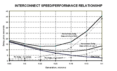
The most widely-used type of IC used today for both processor and memory in PCs as well as mainframes is the complimentary metal oxide semiconductor (CMOS). Traditional CMOSs have been based on aluminum conductors and a silica (SiO 2) dielectric. As devices become faster and more complicated the conductors on the chip must occupy less and less space and therefore become narrower and narrower. This narrowing of the conductor causes an increase in the Resistance-Capacitance (RC) delay. The RC delay, combined with the gate delay, the delay inherent to the logic circuit to which the conductors are attached, is the interconnect delay that controls the speed of the computer. The industry faced a difficult future as it considered devices having conductors less that 0.25 microns in width. From the beginning it was clear that copper would have a decided advantage over aluminum, the commonly used conductor in an integrated circuit (IC). This is due to copper's improved electrical conductivity over aluminum. Copper has about two-thirds the electrical resistance of aluminum. Figure 1 shows the theoretical advantage of copper over aluminum in an interconnect. Hypothetically, a copper and low K dielectric interconnect at 0.1 microns width will offer approximately the same delay as an aluminum and SiO 2 interconnect at the present generation of 0.25 microns width.
 Source: Bohr, Mark T., Interconnect Scaling-The Real Limiter to High Performance ULSI, Proceedings of the 1995 IEEE International Electron Devices Meeting, pp 241-242.
Unfortunately, copper is incompatible with the substrates used in ICs. It has a tendency to migrate into the silicon substrate and thereby poison the system. The task, therefore, became one of designing an IC and a manufacturing process in which the copper conductors were isolated from the metal oxide substrate by a dielectric diffusion barrier.
On September 22, 1997 IBM issued a press release in which they announced a key breakthrough in their CMOS 7S technology using copper instead of aluminum as an interconnect metallurgy. The key to the IBM development was the use of an interface barrier and low permitivity (K) dielectric film-a technology they dubbed the Damascene (or dual Damascene) Process after the art form of metalwork decorated with wavy patterns of inlay or etching. The new technology enables a radical change in chip architecture and employs up to six levels of copper and one local level of tungsten to wire up to 12 million gates, or about 185 million transistors, on a chip compared with 3.4 million gates in IBM's 0.25-micron ASIC (aluminum on SiO 2) process. With the new technology a conductor width of 0.16 microns is possible producing the capability of operating over 400 MHz processor speed.
Following the IBM lead, companies like AMD, Applied Materials, Intel, Lam Research, Novellus Systems, Mitsubishi Electric and Motorola are all jockeying for position in the new technology. All are at various stages in the research and development process for creating the copper interconnects as well as the system used to fabricate the chips and some are already in production. IBM began producing a 32-bit RISC chip, a souped-up PowerPC 750 aimed at high-speed desktop computing in the fall of 1997. IBM's high speed PowerPC processor, using copper interconnect technology, for example, was first used in the 400 MHz Macintosh computer manufactured by Apple Computer, Inc. in March of 1998. Motorola is a close second to IBM in this technology responding to the needs of its major customers-BayNetworks, Cisco, Lucent, Nortel, Ford, 3Com, Ericsson, Nokia and NEC.
According to Novellus Systems the benefits of copper are four fold:
- 1. There is a complexity advantage.
- The higher conductivity of copper simplifies interconnect routing. This reduces the number of interconnect levels from 12 to 6, which removes upwards of 200 process steps and has a direct impact on device yield.
- 2. There is a power advantage.
- Chips with copper interconnect will operate with approximately 30% less power at a given frequency than chips with aluminum interconnect. This technology will enable devices with significantly higher performance for mobile applications.
- 3. There is a cost advantage.
- The semiconductor industry has historically reduced the cost per function by 25% to 30% per year. The reduction in critical process steps with the dual Damascene copper process reduces the overall process cost by 30% per interconnect level.
- 4. There is a speed advantage.
- At 0.13 micron, the interconnect delay for copper and low K materials is approximately one half that of aluminum and SiO 2. Copper is a clear choice at 0.13 micron and smaller because it provides speed enhancement with no sacrifice of device reliability.
The Damascene process, currently the dominant method for working with copper, starts by etching a pattern of interconnects onto a thick layer of dielectric material. A barrier layer is used next to block the copper from diffusing into the silicon, followed by a thin "seed" layer for depositing the copper to create the interconnects. Finally, a chemical-mechanical wash is applied to remove the excess copper. Depositing the copper interconnects on the IC itself is the most difficult part of the Damascene process because the high-aspect ratio features are hard to fill in with out producing voids or cracks.
The diffusion barrier, that prevents copper migration into the silicon substructure, is the key to the successful use of copper as a conductor in ICs. There are a number of opportunities for low K diffusion barriers. Such materials being used are cobalt, chromium, nickel, palladium, tantalum, tantalum silicon nitride, titanium, titanium nitride, silicon nitride, tungsten nitride, tungsten silicon nitride.
According to Sematech, the government/industry electronic research consortium, there are a number of ways of depositing copper on a substrate. Each has its own advantages and disadvantages:
- 1. Electroplating
- Advantages-inexpensive, fast and effective for thick layers.
Disadvantages-concern for general copper contamination in plant, requires a "seed layer" of conductive material (typically sputtered copper), provides a poor step coverage and via filling, also, disposal is a problem to avoid aquatic contamination. - 2. Electroless Deposition
- Advantages-inexpensive (although more expensive than electroplating), and fast, eliminates need for electrodes.
Disadvantages-Poorly characterized and low familiarity. - 3. Physical Vapor Deposition (PVD) otherwise known as "sputtering"
- Advantages-Similar to current processes, well characterized, and offers tremendous metrology/quality control technology.
Disadvantages-Poor step coverage, poor via fill and pinholes. - 4. Metal Organic Vapor Deposition (MVOD)
- Advantages-Good conformality and fill characteristics.
Disadvantages-Expensive and slow, requires specialty organometallic chemicals.
Novellus has developed a complete fabrication solution that will provide the solution of choice for dual-Damascene copper, including barrier layers, encapsulation and equipment that will deposit the copper interconnect itself in a cost effective manner. They have also developed a packaged system for waste-water cleanup.
Applied Materials, a direct competitor to Novellus, who also manufactures the equipment that forms the barrier and seed layers, is working on an alternative to the Damascene process, called the Subtractive Etch Process.
Mitsubishi Electric has developed a hybrid system using copper interconnects for the long distances and aluminum interconnects for the short distances termed System LSI. They plan to begin volume production of System LSI products incorporating this interconnect structure by the second half of 2000.
Clearly, the IBM innovation into the use of copper in place of aluminum has opened an entirely new vista for the computer industry and continual increases in processor speed into the 21st century can be assured.
Also in this Issue:
- Brief Early History of Brass
- Introduction to Brasses (Part I)
- Speeding-up Your Computer in the 21st Century Using Copper ICs
- Spotlight on Copper In Architecture
- Introduction to Brasses (Part II)
- Copper Cleans Up